Deutsche Version dieser Seite
Next:Write Back Unit
Up:Structural and functional description
Previous:Execution Unit
Contents
Stack Memory Unit
The Stack Memory Unit is shown in figure 4.11. Both stack memory and global registers of the microcontroller are located here. To choose a memory cell in the block a base address (which determines the kind of memory access) and an offset have to be provided. Then the base registers or the stack memory is read out (figure 4.12). Which kind of memory cell to read is controlled by a special signal. If it is not set, the offset is added to the data from base register and interpreted as address in stack memory.
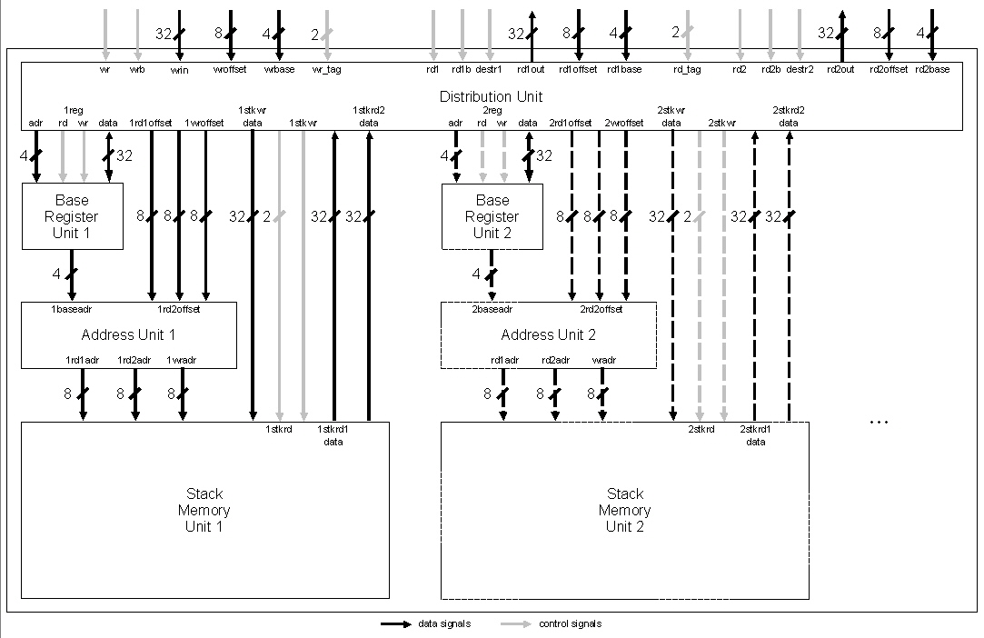
Figure 4.11: Stack Memory Unit
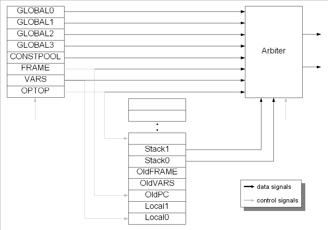
Figure 4.12: Accessing the stack
Two read-ports and one write-port are provided by the stack memory unit. Two is the maximum operand count for one instruction; therefore all operands for the actual instruction can be read at once. To speed up the pipeline and reduce problems with data dependencies the concurrent write access has been added so that a result can be written back and read for execution simultaneously in one pipeline cycle.
Provided by the development environment for implementation of the stack memory unit is only a dual-ported-ram module. It is run with external clock so that all actions can take place in one internal pipeline cycle. This means all four states of the statechart in figure 4.18) will be taken in one pipeline clock cycle.
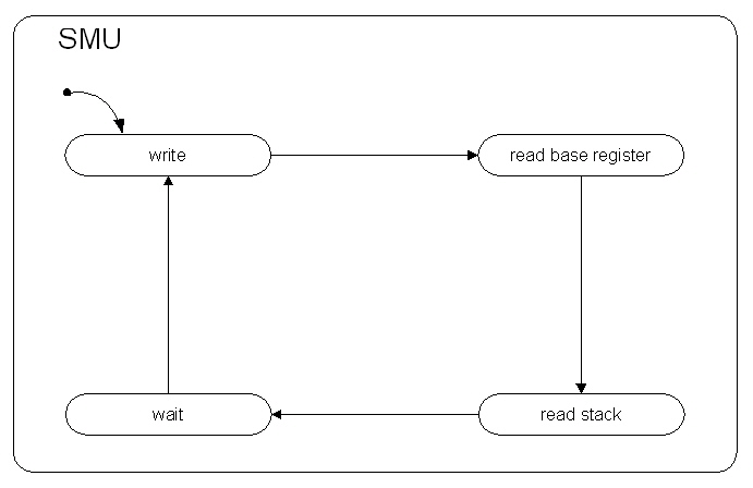
Figure 4.18: Statechart of the Stack Memory Unit
Next:Write Back Unit
Up:Structural and functional description
Previous:Execution Unit
Contents
Robert Zulauf
2000-04-27